Kicad Redux
It's been a few months now since I did the big switch from Eagle to Kicad, so I thought I'd post a few updates on how the process of switching has gone.
I've had to go back a few times to dig old designs out of Eagle, and I can't say that I really miss any features of Eagle. I've gotten very used to all the little graphical glitches of Kicad so these don't bother me as much any more. The designs have definitely gotten a lot better since switching as well.
I commented on the first post about switching I felt Eagle had a better connection between the board and the schematic, but I have to withdraw some of that. There's a few features of Kicad which make a lot more sense now and the connection between the two isn't as bad as I first thought.
For example, it's very easy in Kicad to have both the PCB and schematic up in separate windows on different displays (something I do rather constantly), and this helps make the two feel connected. Highlighting a component on the PCB side will actually cause the schematic to leap and centre that component, so you can see the context both in the board and the schematic very quickly.
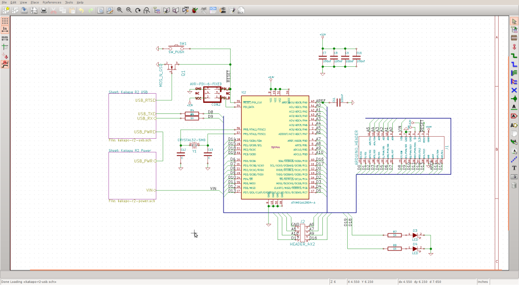
Schematic hierarchies also work really well for breaking a design up into managable chunks. In the image below, I've buried the USB and power sections in their own schematic pages, so it's easy to work on just the relevant parts of the board.
During early PCB layout, the "get footprint" tool is fantastically useful. Hit "T" and enter a reference, and it grabs that part for moving. This makes it far easier to do the initial rough layout with parts in the right order to do things, and makes it easier to find related parts.
The workflow I've gotten very used to now. It's an ingrained routine of change things in schemtic, generate netlist (when annotation usually pops up), adjust the footprints needed in the footprint assignment, and then reload the netlist in the PCB view. It's not quite as fluid as the live connection Eagle has, but it's close enough I'm much more comfortable with it now.
I'm very pleased with the native image to PCB import feature, although it could do with part scaling as currently this really depends on some external tools to get right. But being able to nicely import artwork into the silk as an explicit module is a big improvement over those capabilities in Eagle.
There are still things I'm not happy with about Kicad, but these are more general problems and not enough of a reason to switch back, I genuinely can't see myself switching back to Eagle at all really.
Things that could be better:
- You can't just drop GND vias or even just vias in a spot, at least if you can I haven't found how
- The graphical glitches sometimes can be a bit misleading, is that an extra trace or just noise?
- If you redraw a section of track, it will remove the old section only about 50% of the time. It's not clear to me why it does or doesn't at any given moment.
- In a schematic, if a pin is not on the grid, you can't connect to it. It would be nice if the wires could "snap" to the pin even if it's off-grid
- BOM generation is a bit of a hack and there doesn't seem to be an easy way to generate a consolidated BOM (ie, qty 4 of part X with references R1, R2, R3, R4).
- Refilling zones doesn't appear to have a hot-key. Which means you are forever switching back to the zone tool to refill, and then back again. Grrrr.
All in all, I'm very happy with Kicad and have pushed out about 4 boards now using it, all of which have been just great, and significantly better than previous efforts.
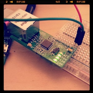
 (another board designed in Kicad)

